Software Radio
* Overview
* Hw_script
* Preload
* Musplay
* Mixer
* Cdman
* Tgt-edif
* fx2_programmer
* Software Radio
* LIGO viewer
* DAQ system
* About me
| x |
Overview
This is a project to create a software radio device that uses USB-2.0 to deliver raw data.
Why software radio ?
Software radio has many advantages:
- CPU can perform a Fourier transform on the captured data and display all active stations instead of having to seek from one to another.
- It should be possible to record multiple channels simultaneously.
- One can use it as a digital scope - an inexpensive alternative to very nice but incredibly pricy Tek scopes.
Goals
- Make a design accessible to determined hobbyist.
- Use only Free Software - this is actually a non-trivial constraint as most large FPGAs require a proprietary place and route tool.
Tasks
- The first task is to verify the delivery method for the captured data. This has been completed - see report here.
- Second task is to build a board with both USB chip and ADC controller and demonstrate analog data capture at reasonable rates. This has been completed - see below.
- New directions ?
- Would be nice to see a PCI Express equivalent to FX2 chip
- There are actually DSP chips with built-in ADC, perhaps build a board with one ?
Other projects
Take a look at gnu-radio webpage for other projects. In particular there is a board designed by Matt Ettus's group that you can buy from Ettus Research LLC website.SR-7.0
SR-7.0 is the latest variant of FX2 chip + ADC board.
Features:
- Two-layer 3" by 3.1" board. I had two manufactured by Futurlec for $30, shipping included.
- Cypress CY7C68013 "FX2" USB 2.0 chip. I used a 100-pin version because it has a wider spacing between pins. They are now starting to produce a newer lower-power version, I might buy these for my next design.
- Analog Devices AD9283 ADC chip directly connected to FX2 GPIF port.
- Ability to use three clocks for ADC ENCODE pin:
- internal FX2 interface clock (IFCLK) (there are two choces, but 30Mhz might not be stable enough)
- FX2 oscillator out pin (CLKOUT) - note that its frequency depends on the speed setting for 8051 microcontroller
- external input
- A connector exposing supply, ground and four ADC pins: IN+, IN-, REF and REFOUT. It is useful for connecting analog frontends to ADC.
- A connector for I2C bus provided by FX2 chip
- The board can work from either USB or external power.
- There are connectors exposing other FX2 input-output ports.
Pictures
The pictures are of SR-7.0i board revision. The PCB files (below) are for later revision, with small bugs corrected (like absence of 100K resistor across USB power pins).
You can click on the images to get full-resolution pictures.
Parts side

- The red and black braided wire connects FX2 CLKOUT pin to FX2 IFCLK and ADC ENCODE pins
- The two jumpers in the top left corner are "SELF POWER" (to use USB power, this one is closest to the USB connector) and "CURRENT" - to make current consumption measurements
- The absent 8-pin IC is the I2C flash chip - I just program FX2 as it comes up with default Cypress USB ids.
- The BNC connector you see on the right is connected to simple 50-ohm "analog frontend" that configures ADC chip for single-ended operation (it is described in the ADC datasheet). This is convenient for connecting to test equipment like signal generators.
- This layers is marked as "SOLDER SIDE" in PCB layout. This is because I was concentrated on getting connections to surface mount chips that are on the other side.
Surface mount side

- You can clearly see CY7C68013 "FX2" chip, AD9283 ADC chip and the 3.3V voltage regulator LTC1763 made by Linear Technology
- The toughest part of making this board was soldering the FX2 chip. I wish they came out with a package with larger pin spacing !
- Earlier board revisions used MAXIM ADC's - these have even tighter pin spacing than FX2 and, as you can imagine, this did not work out that well.
- When I first assembled the board it did not work - which was in stark contrast to the SR-1 project I assembled earlier. After much tinkering it turned out that if I press on FX2 chip hard enough it would show itself to USB bus. Presumably poor connections were to blame. I redesigned the board to allow for longer pads so it is easier to solder, but it is still tricky.
- The little "1" markings show where the first pin of the IC is, so it is easier to place them correctly.
- Note that the USB connector is on the other side.
Screenshot

- This screenshot shows fx2_viewer (part of fx2_programmer) displaying waveform and Fourier transform in real time.
- Since, like fx2_programmer, fx2_viewer uses libusb for input/output I have not been able to get more than 9 MB/sec - this is less than my best number benchmarked before. Probably something inside Linux kernel or libusb has changed since.
- The firmware running inside FX2 is available from CVS, module 8051, subdirectory SR-7.
Making your own
I have not bothered to make a schematic as the design is a straighforward combination of FX2 ATA evaluation board (chop off ATA connector) and AD9283 evaluation board (chop off all ICs except AD9283).
I did, however, write a bunch of Tcl/Tk scripts that serve a similar function (have a description of all connections) and produce a preliminary layout for PCB. You can think of them as a "TeX for boards" (note: it is *not* as easy as LaTeX so some tweaking is required to position parts and make traces).
The SR-7.0j PCB layout was created with the wonderful PCB program. Futurlec had no problem producing it from Gerber files generated by PCB. Note: I did not order silk screening, so it is somewhat screwed up on the board layout - overlaps parts, etc.
Here are some notes on board assembly in case anyone wants to tinker with their own board:- First, take a bare USB connector, hook it up to the cable and find the power supply pins. Your multimeter should show 5 V
- Insert the connector into the board and check that you can see the voltage where they are supposed to be (i.e. that ground is ground). If all is ok solder the connector into place and check that it is correct and the computer does not complain about over-current conditions on USB ports (which would indicate a short).
- Solder the parts for voltage regulator LTC1763. These are
- REG_SWITCH jumper (short it to use USB power)
- Voltage regulator REG (watch for pin 1)
- Capacitors C17 (0.01 microFarad - exactly), C18 (about 4.7 microFarad), C16 (about 6.3 microFarad)
- LED network: POWER_LED (use a small current LED) and R6 (1K) (you might want just to insert LED first to make sure the polarity is right)
- Time for bravery ! We are going to solder FX2 chip parts:
- Crystal oscillator: XTAL, capacitors C8 and C9 (22pF each)
- I2C network resistors R10 (1K) and R12 (10K) - without these FX2 will not enumerate properly
- Reset and wakeup networks: R2 (100K) , R5 (10K), C12 (0.1 microFarad)
- Bypass capacitors C3, C20, C1, C19, C2 - use ceramic ones about 0.1 microFarad each. I suggest not
soldering all of them at once to leave space for higher (or lower) value ones in case they are needed.
However, solder at least C3, C20 and C19. - Position FX2 chip - make sure first pin is correct. Solder pins on oppossing ends and then do the rest.
- I found convenient to use a very fine-tip soldering iron at around 275 Celcius. Just tin it and touch at the butt end of the pin until the solder melts underneath. It would help if there is a tiny bit of solder on the iron tip itself.
- If you get solder stuck between FX2 pins just bruch with the iron tip away from the chip making sure to melt the stuck bit and clean iron tip from solder between tries.
- When all done connect the device to USB port and check that it enumerates correctly. You can also play with FX2 chip using some of the 8051 scripts in CVS.
- Once you know that FX2 chip is working right, solder on the rest.
- solder the connectors for ADC, FX2 D and C ports, CLKSWITCH
- Solder R3 (10K) and R4 (100K) resistors - they make sure ADC is powered down when the board is first plugged in
- Solder capacitor C8 (0.1 microFarad)
- Solder the rest of bypass capacitors - this does not hurt.
- You can omit the drossel L1 - it is there to provide additional isolation for ADC analog supply. I found out it is not necessary.
- Position AD9283 chip, check that pin 1 is where it is supposed to be. Solder opposing pins first. You will find this much easier than soldering FX2 chip.
- There is a place solder EEPROM (or better yet - an IC socket for EEPROM), I did not bother with this.
- To test ADC operation you would need to program FX2 with appropriate firmware. You can find the one I used in CVS, module 8051, subdirectory SR-7. Make sure to place a jumper connecting IFCLK FX2 pin to ENCODE input of ADC. (use CLKSWITCH block). You might also want to connect CLKOUT FX2 pin to IFCLK and ENCODE (see pictures).
Parts list
- CY7C68013 "FX2" chip - probably the most expensive part in the design. You might want to replace it with pin-compatible lower-power version (see Cypress website).
- AD9283 ADC chip
- LTC1763 3.3V voltage regulator
- Connectors: USB B connector, single and double row headers. I suggest you also get some BNC socket connector (you might want to get several). Get also some RG58 BNC plugs and RG58 cable to match them. Of course, the choice of RF connector is somewhat arbitrary :)
- 24 Mhz crystal as described in FX2 datasheet
- Several resistors: 1K, 10K, 100K. You would want 50 ohm and 25 ohm resistors for the simple ADC frontend.
- Several ceramic capacitors: 22pF, 0.1microFarad, 0.01 microFarad.
- A couple of electrolytic capacitors: 4.7microFarad, 6.3microFarad. You can use tantalum if you like.
- A small current LED - use one that lights up at 3mA.
- A stock USB 2.0 cable (plain USB 1.1 might not work right).
Frontends
So far I only have a hastily sketched schematic of 50 ohm BNC frontend and photodiode one. Hopefully this gives some idea of how to use the board. I'll post more as they become available (perhaps learn to use gschem along the way).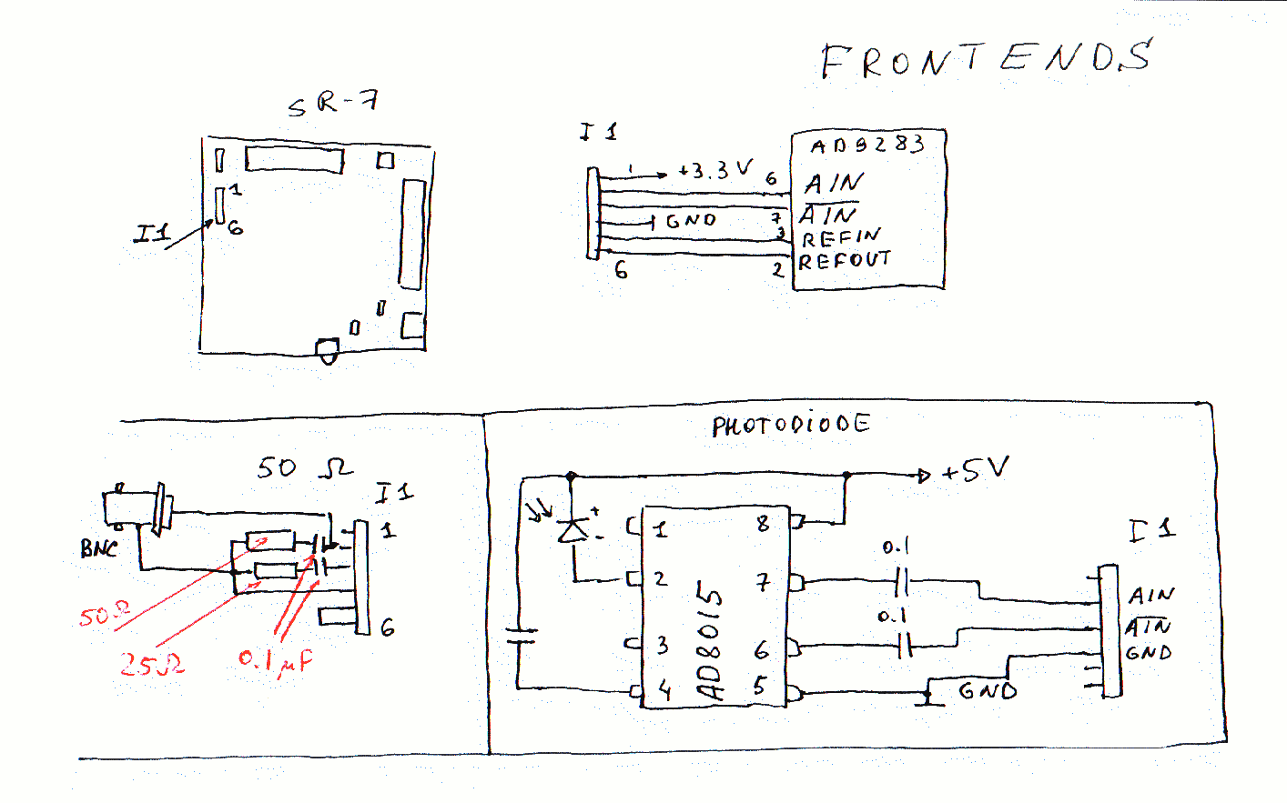
Links and References
IC manufacturers
- Analog devices website
- Cypress Semiconductors website
- Linear Technology website
- National Semiconductors website
- Maxim/Dallas Semiconductors website
Open Source Tools
- PCB - a pcb layout program
- SDCC small device C compiler website
- libusb website
- Linux USB implementation website
- fx2_programmer website